Badboys/alphagamma
Alpha and Gamma Cawinkadink
Barrett Nibling, Adolfo Gomez, Micheal Bouchey
March 20, 2008
Contents |
Abstract
abstract here
List of Figures
- Figure 1 - Experimental Setup
- Figure 2 - Wiring Diagram
Introduction
In many radioactive decays, the initial alpha or beta emission isn't the last. In other word, The decay will go to another excited state as opposed to ground state. These states tend to have half-lives in the magnitudes of picoseconds or femtoseconds. In this experiment, we used the 59 keV excited state in 237-Np to demonstrate this. In this state, there is a high populous, via alpha decay, of 241-Am. Which in turn will give a low energy gamma decay with a half life of approximately 70 nanoseconds. Therefore, the general purpose of this lab will be to determine and measure this gap of time to prove coincidence occurs. In order to time this, we will set up timing system using various electronics, such as the Timing Single Channel Analyzer (TSCA), which produces a fast pulse whenever a signal is received becoming the start and stop signals; and the Time to Amplitude Converter (TAC), which will be our stop watch, using the stop and start signals from the TSCA.
Theory
Radioactive Decay
In this experiment, the primary and secondary decay processes (decay chain) of parent isotope 241-Am are recorded using detectors, timing, coincidence, and amplification electronics. With a half-life of 432.2 years, 241-Am is the second most stable isotope of Americium, next only to 243-Am. The primary alpha decay of 241-Am results in an excited state of the stable 237-Np isotope. The excited 237-Np undergoes isomeric transition, undergoing low energy gamma decay with a half-life of approximately 70 ns. The 241-Am alpha decay provides the start signal for the timing measurement, while the 237-Np meta-state decay provides the stop signal.
Detectors, Timing, Coincidence, and Amplification Electronics
A scintillator detector is best suited for low energy gamma detection since this form of radiation does not carry a charge. Incident gamma radiation interacts with electrons in the scintillator crystal, transferring energy to the electrons. The electrons subsequently de-excite, leading to the production of many low-energy photons. The photons are collected through a photomultiplier tube, the signal is then amplified and digitized.
A modest array of detectors and electronics are used in this experiment to capture and record data. For high energy alpha decays, a semi-conductor charged particle detector is used because of its applicability to a wide range of energies. In this instance, a Silicon detector is used to measure the alpha particles emitted by the 241-Am source. The incident radiation releases charged carriers in the detector, resulting in a transfer of electrons from the valance band to the conduction band. The resulting holes in the valance band and carriers on the conduction band travel to electrodes, under influence of an electric field, where a signal can be gathered and measured by external circuitry.
The experiment also requires the use of sophisticated electronics. The detectors signals are amplified and sent through two NIM modules for analysis. The first NIM module is a Timing Single Channel Analyzer (TSCA) which produces a standard pulse (negative or positive) for each analog signal received. The TSCA module also provides a means for segregating unwanted signals. By setting a pulse height window, the TSCA converts only analog pulses within the range specified.
The second NIM module is used to analyze the delay between TSCA signals. The Time to Amplitude Converter (TAC) accepts a start and stop input signal, semiconductor detector signal and scintillator detector signal respectively, and converts them into a pulse with a height proportional to the time elapsed between signals.
Finally, the TAC signal is collected an analyzed through an Analog to Digital Converter/Multichannel Analyzer system (ADC/MCA). A computer system and Maestro software is used to collect and graph data. The software takes data and organizes them in bins corresponding to the energy level of the signal.
Procedure
1. Build a vacuum system (using one aluminum cube) with a port for a semiconductor detector on one end and a port for a radioactive alpha source on the opposite end. Connect the cube the existing pumping setup (Fig. 1).

Fig. 1 - Experimental Setup
2. The semiconductor detector is mounted on a special extension to bring it near the alpha source position on the other side in vacuum.
3. The 241-Am source is mounted with a special flange that has an outside port fir the low energy gamma detector. This detector has a relatively small crystal optimized for the approximately 60 keV gamma rays encountered in this experiment.
4. Close and evacuate the system with the roughing pump (to about 7 mTorr).
5. Connect: preamplifier to semiconductor detector feed-through: preamp output T to oscilloscope; preamp power to the outlet at the back of the amplifier. Power up the NIM bin. Connect the high voltage cable to the NIM HV power supply. Monitor the electric noise level of the amplifier signal on the oscilloscope while slowly turning the voltage up to +40 V. Describe what you see. Describe and sketch the signal seen on the oscilloscope: risetime, falltime, noise.
6. In order to shape and amplify the signals further for data acquisition, connect the preamp output to the amplifier input. Select the correct polarity on the polarity switch. Connect the unipolar output to the oscilloscope. Describe and sketch the signal seen on the oscilloscope: risetime, falltime, noise. What changes with using the gain switch and the shaping-time switch? Adjust the gain to a signal of 6 V for the highest alpha energies.
7. Startup the data acquisition program for the PC. Connect the unipolar output of the amplifier to the ADC/MCA input. Start the data acquisition and take a spectrum of the 241-Am source signal. Save for future printout on floppy disk.
8. Mount the scintillation detector in the slot prepared for it. This detector has a built in photomultiplier base (base) connected to the photomultiplier (PM).
9. Connect the signal output cable of the PM base to the oscilloscope. Check for a signal.
10. Connect the high voltage (HV) input cable of the PM base to the HV output of the HV power supply.
11. Turn on the HV power supply. Try to see the signals by adjusting the voltage in +100 V increments. Do not exceed +1200 V.
12. Take notes of the results and sketch the signals visible on the oscilloscope at +1000 V. Describe and sketch the signal seen on the oscilloscope: risetime, falltime, noise.
13. Connect the signal to the spectroscopy amplifier input. Check input signal polarity.
14. Connect the oscilloscope to the amplifier output (unipolar). Sketch the signal.
15. Connect the unipolar output with the ADC/MCA input and start a measurement. Adjust the amplification so that you can clearly see the signal peak in the spectrum. Save to disk for future printout. Sketch the spectrum. Check the signal again on the oscilloscope. Record the voltage of the photo peak.
16. Connect the output of the semiconductor amplifier to the input of the TSCA. Check with the oscilloscope if negative output pulses are produced.
17. Connect the bipolar output of the scintillator amplifier to the input of the other TSCA. Check again with the oscilloscope if negative output pulses are produced.
18. Connect additionally the unipolar output of the amplifier to the oscilloscope and trigger with the TSCA output. Try to set the TSCA window on the dominant approximately 60 keV signal. Introduce a delay into the TSCA and record the effect.
19. Connect the semiconductor line TSCA output to the start input of the TAC. Check with the oscilloscope if a valid start signal is registered.
20. Connect the scintillator line TSCA output to the stop input of the TAC. Select a 2 μs delay time at the TSCA. Select a full-scale time range of 10 μs at the TAC.
21. Monitor the TAC output on the oscilloscope. Describe and sketch it.
22. Connect the TAC output of the ADC/MCA and take a spectrum for approximately 1 hour. The final setup should be wired according to Fig. 2 below.

Fig. 2 - Wiring Diagram
23. Save the spectrum onto floppy disk for future printout and analysis.
24. In order to calibrate the time spectrum, introduce and additional delay in the form of a long cable or a NIM module in the scintillator line between TSAC ad TAC.
25. Take another spectrum for about one hour.
Results
Data here
Results 1
Example Table
The First Order Spectrum:
| Color | θdiff (degrees) | λ (nm) | Error (nm) | Published λ (nm) | |
|---|---|---|---|---|---|
| Purple | 15.6 | 448.0 |  2.0 2.0
|
447.148 | |
| Teal | 16.4 | 470.3 | 2.0
|
471.314 | |
| Green | 17.2 | 492.6 | 2.0
|
492.193 | |
| Green | 17.5 | 500.9 | 2.0
|
501.567 | |
| Yellow//Orange | 20.7 | 588.8 | 2.0
|
587.562 | |
| Red | 23.6 | 666.9 | 2.0
|
667.815 | |
| Dim Red | 25.1 | 706.7 | 1.9
|
??? |
Results 2
Error Analysis
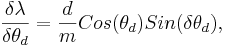
For the error analysis, there are two variable associated with an error, θd and θi.
The partial errors for each of the variable are calculated from the formulas
and,
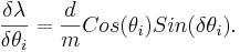
Then the total error is the sum of the two partial derivatives added in quadrature,
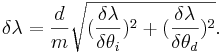
The values for δθd and δθi used are half the value of the smallest unit of measure on the device, .05 degrees.
Conclusion
conclusion here
References
[1]
[2]